عضویت
عضویت  ورود اعضا
 راهنمای خرید


P055_50W-200W_Planar Transformer_en0 pages
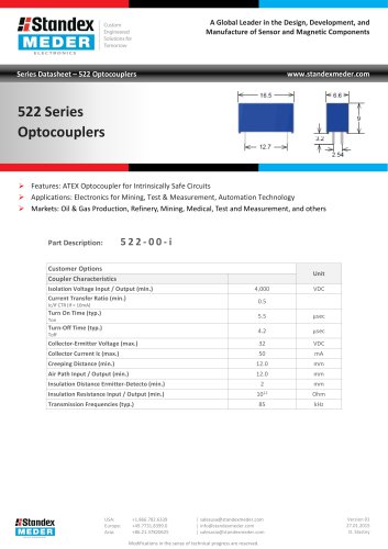
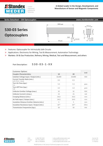
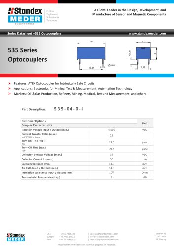
DESIGN GUIDE Planar Transformers & Inductors
ff'Standex | Custom Engineered |
Solutions for Tomorrow | |
ELECTRONICS |
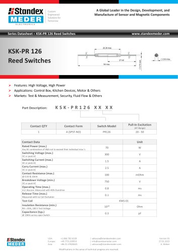
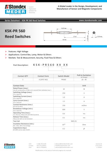
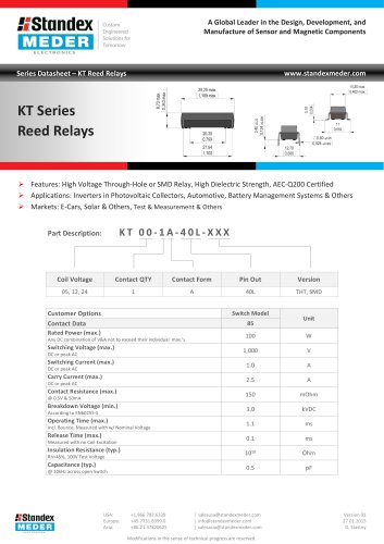
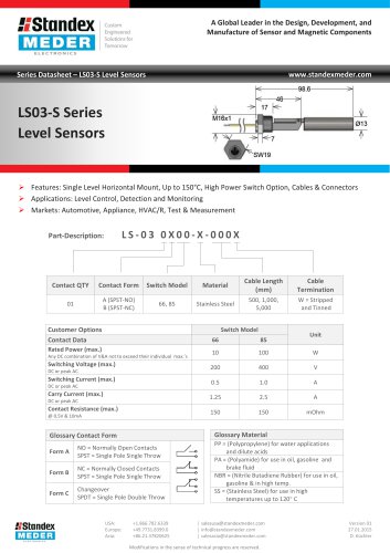
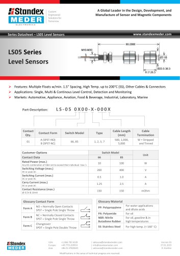
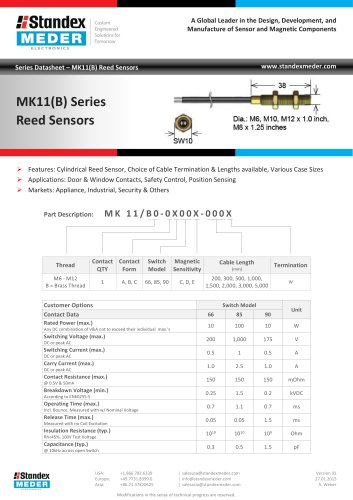
SIZE P055
Power Range 50W-200W
"Application Engineering Experts" □ | |||
CUSTO | M | S STANDARD | |
CO
111
<
X
HI
CD
CO
111
Q
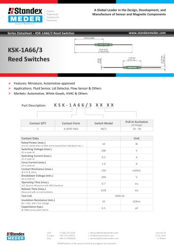
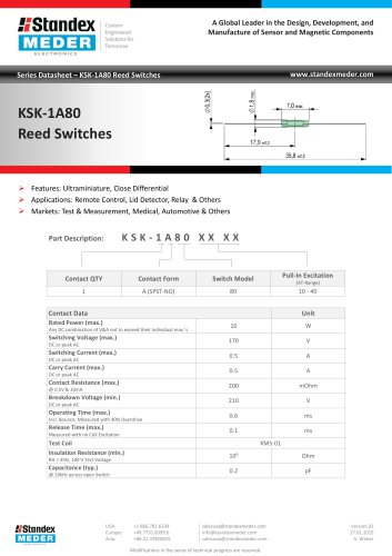
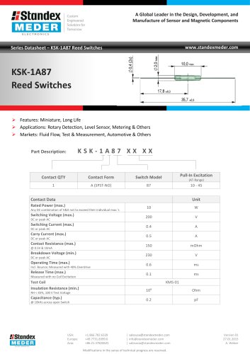
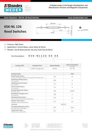
Design Input Pri. Np Sec. I Out. Sec. Ns1
Example Voltage Turns Ns1 Max (2) Turns
Part# VDC (Pins) VDC ADC (Pins)
Sec. Sec. Height
Ns2 Ns2(3) mm(in)(1)
VDC Turns Typ.
1250-1 36-75 8 2.2 50
1250-2 18-36
1250-3 36-75 12 3.3 35
2.2 50
1250-6
1250-7"
1250-4 18-36 6 3.3 40
1250-5"" 36 - 75""" ¥ ¥ 56""
18 "36 """V ¥ 56""
36 - 75"""¥ i 2 "" 125"
1250-8 18 - 36""" 4" i 2 "" 12. 5"
1250-9" "266-356"" "48 28 ¥""
1256-l"6"266-356"" "48 48""" 2_.¥"
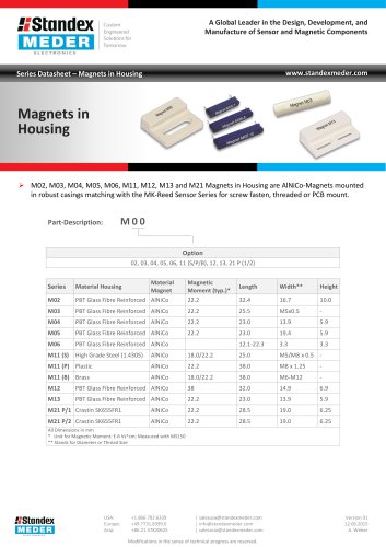
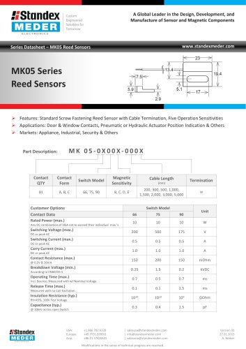
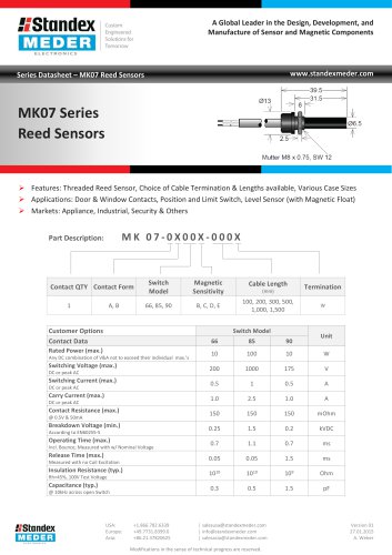
P055 ALTERNATE DESIGNS
1284-{""¥6"- 75 """l6 "-" i¥"
1 "284-2"" 18 -¥¥"""¥ "-" i¥"
1
.....
.....
.....
.....
.....
.....
.....
"12"
"24"
9.1 (0.360")
""9".l"("o".366")"
" ~9£(6.3&y)
" 9".6"(b".586;;)"
" 9".6"(b".586")"
""9".6"("o".386")"
" ~9£(6.3&y)
""9".6"("o".386")"
"T677 (6.420")
"i6"7(6.42"d"j
Notes: Full electrical, thermal, and efficiency calculations available upon request 1) Length (L) may
vary depending on terminals. Height (H) may vary depending on input / output requirements. 2)
Estimated value for normal conditions. Current rating can be up to 30% higher for through hole
applications. 3) Ns2 / Ns3 max. load current output after rectification by (turns) as follows: (8) = 2.5
A each, (7) = 3.0 A each, (6) = 3.5 A each, (5) = 4.5 A each, (4) = 5.75 A each, (3) = 7.5 Aeach, (2)
= 10.0 A each
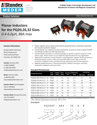
Highlights
• Patented (U.S. PAT. 7,129,809) design with superior
thermal management
• High efficiency (low losses), ultra compact, low-profile
• Great co-planarity of terminals due to patented header
offering repeatable height
• Excellent solderability (Pb-free or Pb/Sn Solder)
• Standard sizes / customer configurations
• Quick custom turn-around often without start-up or tool-
ing costs
• Inductors available for design in all packages
Customize beyond these examples!
Rated power 50W-200W/ Frequency range 175-300kHZ
Surface mount (SMD) or through hole (TH)
Topology - Half Bridge, Forward (w/active rest), Flyback
Current rating max. SMD=20A, TH = +30%
Isolation voltage pri-sec/pri-core 500-2,000VDC
Soft switching, single or multiple outputs
Different switching frequencies, input/output voltages
Primary turns - other number (no fractions)
Secondary Ns1, Ns2 / Ns3 turns 1- 8 (no fractions)
Thermal solutions heat sinks, etc.
SURFACE MOUNT DESIGN
9.0
6.0
3.0
C/L -
3.0
6.0
9.0
PCB Pad Layout
All Pad dimensions tolerance +/- 0.1
30.5
\|/14pl.
2.3
5.1
<->
Notes
1. Dimensions are in mm 4. Header: LCP, natural color
2. Drawing not to scale 5. Pins: Copper
3. Tolerance +/- 2% unless noted 6. Pin Finish: Tin (Sn) over Nickel (Ni)
21.8 mm
n n n n n n
t=t; ig] (a) (nb) (a) ifB) (a
fiStandex
IEDER1
ELECTRONICS
U.S. PAT. 7,129,809
These models are for reference only and may NOT exactly match the design examples provided.
8
Fill out a design request today! | meder.com/planartransformers.html
"